A Microelectronics Commons regional innovation hub
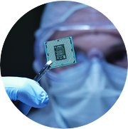
Capabilities and tools
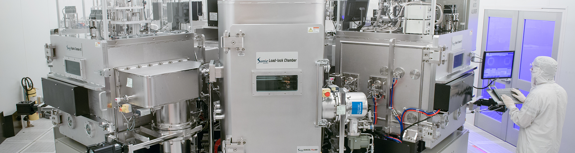
World-class capabilities and expertise
SWAP Hub members have access to cutting-edge physical and virtual tools and world-class expertise across their workflow — from prototype design to demonstration — in high-demand capability areas.
SWAP Hub capability areas
Led by ASU and Sandia National Laboratories

Rad-hard CMOS+X integration
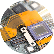
Heterogeneous integration
Circuits, architectures and test

Metrology and characterization

Power and RF electronics

ASU key capabilities
- Macrotechnology Works, a 250,000 square foot facility with 49,000 sqft cleanroom, 22,000 sqft wet/dry labs with substantial H6 capability
- Materials-to-Fab Center, a groundbreaking partnership with Applied Materials bringing cutting-edge 300mm industry tools for materials development at scale
- ASU Core Research Facilities for advanced research, consultation and project execution with ASU’s experienced, professional engineering staff
- Industry scale operations utilizing 300 mm tools to develop, characterize and optimize new materials and processes for FEOL as well as advanced packaging leveraging Deca Technologies FOWLP M-Series™ and Adaptive Patterning technology
- Vast network of Extreme Environment testing capabilities
- Diamond Lab fabricating the highest current RF devices in the world
- Trusted and Assured services ranging from threat assessments related to side-channel leakage and fault injection, through hardware-based security IP integration including physical unclonable functions, secure boot, hardware-based authentication protocols and differential power analysis countermeasures

Sandia key capabilities
- The Microsystems Engineering, Science and Applications (MESA) Complex and the Center for Integrated Nanotechnologies, two conjoined 200 mm Si (180 nm) and 100 mm III-V capable compound semiconductor fabs
- Co-located R&D and production at largest government-owned microfabrication facility
- Entirely export-controlled, secure and capable of handling classified material
- Low volume, high work mix offers high flexibility and agility
- Capabilities for heterogeneous integration
SWAP Hub’s three cross-cutting themes
Trusted and assured
The hub’s project performers are committed to designing, testing and validating the security and trust of microelectronics from IP design through fabrication, packaging, testing and distribution.
Rad-hard/extreme environment reliability
Going beyond conventional commercial approaches, the hub’s projects address potential threats to electronics that operate in space and other extreme radiation environments to guarantee functionality and reliability.
Workforce development
The hub produces microelectronics talent tailored to DoW-identified needs through partnership with industry, higher education institutions and nonprofit organizations.

Learn more about our capabilities and themes
High fidelity execution and innovation
The SWAP Hub leverages ASU’s sophisticated, mature management systems for working with industry and DoW clients, as well as its extensive experience in managing large-scale federal projects and complex subawards. ASU ensures DoW and industry-level rigor in management of SWAP projects through a systems-based manufacturing approach and quality systems model that enables agility and innovation while guaranteeing fidelity and trusted, secure collaboration. Additionally, ASU maintains capabilities to carry out classified work, allowing the hub to execute projects that require security clearance.

Split-fab innovation for end-to-end success
The SWAP Hub leverages a unique “split fab” relationship between Arizona State University and Sandia National Laboratories, enabling a unique synergy of capabilities.
Sandia specializes in fabrication of radiation-hardened CMOS wafers with front-end-of-line process steps at its Microsystems Engineering, Science and Applications Complex and Center for Integrated Nanotechnology. ASU handles back-end-of-line processing customized for CMOS+X at its MacroTechnology Works semiconductor fab.
The SWAP Hub also leverages more than $500 million in investment from the private sector and the state of Arizona, including $270 million from ASU, Applied Materials and the Arizona Commerce Authority for the new Materials-to-Fab Center at ASU’s MacroTechnology Works.
Capability and theme details
Rad-hard CMOS+X integration capability
SWAP Hub is developing a CMOS Discovery Platform that will allow hub users to heterogeneously characterize integrated BEOL device arrays under baseline and radiation environments. In addition, the Discovery Platform supports the integration and array-scale characterization of emerging devices by offering a unique, interposer-based option. In this case, emerging devices are fabricated on a large, planar substrate that is compatible with typical university labs, and supports micron and nanoscale devices processed under nonideal processing conditions.
Capability co-leads

Sapan Agarwal
Principal Member of Technical Staff, R&D, Sandia National Laboratories
Rad-Hard CMOS+X Integration, Co-Lead

Matthew Marinella
Associate Professor, School of Electrical, Computer and Energy Engineering, Arizona State University
Rad-Hard CMOS+X Integration, Co-Lead
Heterogeneous integration capability
Heterogeneous integration refers to the integration of separately manufactured active and passive electronic components using advanced semiconductor packaging technologies. Within the Swap-Hub we have access to a wide range of packaging technologies which includes a world leading fan-out-wafer-level prototype line based on the DECA MSeries Gen2 platform. In addition to this our packaging capabilities are supported by accelerated life tests such as HALT/HAST, HAST and thermal cycling as well as advanced multiphysics analysis tools for thermal management and physics-of-failure reliability assessments.
Capability lead

Christopher Bailey
Professor, School of Electrical, Computer and Energy Engineering, Arizona State University
Heterogeneous Integration Capability Lead
Circuits architectures and test capability
The circuits and architectures design and test capability area aims to provide design, tapeout, and test support for the SWAP Hub activities and projects. The SWAP Hub will establish and maintain a circuit Intellectual Property (IP) library that contains common digital, analog, and RF circuit blocks, such as computation cores, multipliers, chip-to-chip communication units, analog-to-digital converters, power management units, RF amplifiers and mixers, and oscillators. The IP library will be a hybrid of soft IP (defined at the register transfer level) and hard IP (defined by layout targeting a specific technology node). Additionally, the SWAP Hub circuit testing laboratory contains multiple test equipment units, including signal generators, signal analyzers, and high speed oscilloscopes that are available to the hub member for a usage fee.
Capability lead

Sule Ozev
Professor, School of Electrical, Computer and Energy Engineering, Arizona State University
Circuits, Architectures, and Test Capability Lead
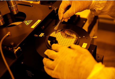
Metrology and characterization capability
The primary goal of the Metrology capability of SWAP Hub is to integrate existing and emerging materials characterization techniques to enable a rich suite of methods in support of yield, reliability, and failure analysis for the projects in our pipeline.
Capability lead

Umberto Celano
Associate Professor, School of Electrical, Computer and Energy Engineering, Arizona State University
Metrology and Characterization Capability Lead
Power and RF electronics capability
The RF + Power Capability Area of the SWAP Hub provides growth and fabrication expertise for the prototype demonstration of ultra-wide bandgap (UWBG) devices based on diamond, boron nitride, aluminum nitride and gallium oxide. Material properties (carrier concentration, mobility, resistivity etc.) can be extracted by Hall effect measurements up to 500C. High-voltage/high-current (3 kV/100 A) I-V and C-V measurements can be automated with a FormFactor probe station for sample sizes ranging from pieces to 300 mm wafers. A similar FormFactor probe station for RF measurements allows automated on-wafer DC and small-signal parameter extraction up to 110 GHz.
Capability lead

Trevor Thornton
Professor, School of Electrical, Computer and Energy Engineering, Arizona State University
Power and RF Electronics Capability Lead
Trusted and assured theme
The Trusted and Assured (T&A) Theme provides a set of cross-cutting area capabilities for assessing, enhancing and validating security and trust within microelectronic systems. The T&A infrastructure provides capabilities that allow SWAP Hub participants (i) to assess threats and vulnerabilities within their prototypes, (ii) to integrate security enhancing IP, (iii) to utilize security assessment point tools within EDA tool flows, and (iv) to carry out assessment activities on abstract models of the prototypes, and on fabricated prototypes. Assessment facilities including an FPGA test bed for prototype emulation, as well as oscilloscopes, source-measure-units, automatic test equipment and physical inspection equipment, are available for assessing side-channel leakage and physical and functional vulnerabilities for a usage fee.
Theme lead

Jim Plusquellic
Professor, Electrical and Computer Engineering, University of New Mexico
Trusted and Assured Theme Lead
Rad-hard/extreme environment reliability theme
SWAP Hub efforts conducted under the Extreme Environments theme address potential threats to electronics that operate in space, strategic or other harsh environments. The environments include settings where radiation (e.g., heavy ions, neutrons, electrons, protons, gamma- & x-ray, and microwave), temperature, or other external conditions pose threats to electronic function and reliability not considered by the commercial microelectronics industry
Theme lead

Hugh Barnaby
Professor, School of Electrical, Computer and Energy Engineering, Arizona State University
Rad-Hard/Extreme Environment Reliability Theme Lead
Workforce development theme
SWAP Hub’s workforce development mission is to enable a robust, thriving microelectronics industry in the Southwest USA. We enable this by investing in enhancing academic programs aligned with the needs of the microelectronics industry, upskilling and reskilling opportunities for working professionals, digital/virtualized learning experiences, and raising awareness among K-12 students and regional communities for career pathways in microelectronics.
Theme lead
